 Have you been wondering what the Apple iPad looks like inside? The FCC have taken one apart to make sure it clears their tests and have posted the images on-line. One thing to note here is that this FCC teardown is no where near as in depth when compared to the one iFixit will do tomorrow, but it’s still interesting to see what’s going on in there including how much actual space there is available even though it contains a massive set of batteries.
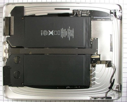
The picture above shows the back panel (the screen rests on top of this) whereby the two large brick shaped objects are the batteries that keep it powered for 10+ hours. You can also see the dock connector running across the batteries and see that it’s slightly unfastened from the bottom edge of the iPad.
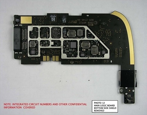
One of the images below shows the main circuit board that contains the brains that run this thing… ie the A4 chip although specific chip numbers have been covered up I guess to protect their identity before the launch… again, iFixit no doubt will reveal all chip numbers associated with the iPad.
I have to say I am quite surprised about the lack of space used by the components. I guess we get used to seeing smartphones where ever last mm has something crammed in to it. Having a larger form factor certainly does have it’s benefits and Apple have done a great job at packing everything in there. It’s interesting to note that there is actually space for a camera and other items that could be used, perhaps in an iPad 2nd gen though.


Via: Giz


from inside the iPad looks better!! 😉